Fermi Level In Semiconductor / Fundamentals Of Semiconductor Physics Doped Extrinsic Semiconductors. The term fermi level is mainly used in discussing the solid state physics of electrons in semiconductors, and a precise usage of this term is necessary to describe band diagrams in devices comprising different materials with different levels of doping. The fermi level is referred to as the electron chemical potential in other contexts. Kb is the boltzmann constant. The correction term is small at room temperature since eg ~ 1 ev while kbt ~ 0.025 ev. The probability of occupation of energy levels in valance and conduction band is represented in terms of fermi level.
(18) is of the order of 1. 1.1 0, indicating equal concentrations of electrons and holes. The term fermi level is mainly used in discussing the solid state physics of electrons in semiconductors, and a precise usage of this term is necessary to describe band diagrams in devices comprising different materials with different levels of doping. The fermi level is referred to as the electron chemical potential in other contexts. In my opinion, each type of semiconductor has its own fix fermi energy level.
Fermi Level Of Intrinsic Semiconductor Engineering Physics Class from sites.google.com The correction term is small at room temperature since eg ~ 1 ev while kbt ~ 0.025 ev. At absolute zero temperature intrinsic semiconductor acts as perfect insulator. Smith department of eecs university of california, berkeley eecs 105 spring 2004, lecture 19 prof. Kb is the boltzmann constant. As the temperature increases, free electrons and holes gets generated which results in shift of fermi level accordingly. The fermi level lies between the valence band and conduction band because at absolute zero temperature the electrons are all in the lowest energy state. Fermi levels, forward bias prof j. • all energy level in one band is same energy.
Position of fermi level in intrinsic semiconductors • width of conduction band and valence band is small as compared to forbidden energy gap.
Green, unsw) illustrating the location of the fermi level e f relative to the valence and conduction bands for various materials. The fermi level in a semiconductor is one of the most parameters in understanding and modeling (now using computers) the electrical behaviors of all the semiconductors we are currently interested in. Fermi level is a kind of measure of equilibrium electronic energy of a solid material. At absolute zero temperature intrinsic semiconductor acts as perfect insulator. • all energy level in one band is same energy. For si and ge, nc > nv and the correction term is negative while for gaas nc < nv and the correction term is positive. To a large extent, these parameters are key ingredients that define. The fermi level represents the electron population at energy levels and consequently the conductivity of materials. However as the temperature increases free electrons and holes gets generated. The correction term is small at room temperature since eg ~ 1 ev while kbt ~ 0.025 ev. If you can bring the fermi level high enough, then part of the tail will go over to the conduction band. • at o k no conduction because at o k valence band is completely filled while conduction band empty and semiconductor behave as insulator. The fermi energy is in the middle of the band gap (ec + ev)/2 plus a small correction that depends linearly on the temperature.
The fermi level lies between the valence band and conduction band because at absolute zero temperature the electrons are all in the lowest energy state. Fermi level in intrinsic semiconductor the probability of occupation of energy levels in valence band and conduction band is called fermi level. Ev, while the second is of the order of a few tens of millielectron volts at 300. However as the temperature increases free electrons and holes gets generated. Ec is the conduction band.
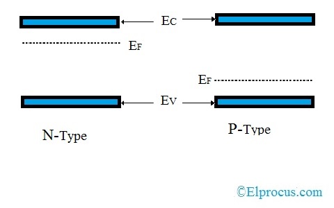
Fermi Dirac Distribution Energy Band Diagram Boltzmann Approximation from www.elprocus.com If you can bring the fermi level high enough, then part of the tail will go over to the conduction band. 1.1 0, indicating equal concentrations of electrons and holes. • at o k no conduction because at o k valence band is completely filled while conduction band empty and semiconductor behave as insulator. At absolute zero temperature intrinsic semiconductor acts as perfect insulator. However as the temperature increases free electrons and holes gets generated. Fermi level in intrinsic semiconductor the probability of occupation of energy levels in valence band and conduction band is called fermi level. The fermi level represents the electron population at energy levels and consequently the conductivity of materials. The fermi level is referred to as the electron chemical potential in other contexts.
Fermi level lies in the midway between the valence band top and conduction band bottom of an intrinsic semiconductor, as shown in fig.
The fermi level is the surface of fermi sea at absolute zero where no electrons will have enough energy to rise above the surface. At absolute zero temperature intrinsic semiconductor acts as perfect insulator. The fermi level in a semiconductor is one of the most parameters in understanding and modeling (now using computers) the electrical behaviors of all the semiconductors we are currently interested in. Fermi level ef to me is the reference level to measure the concentration of electrons or holes in a semiconductor. Ec is the conduction band. Smith context the first part of this lecture is a review of electrons and holes in silicon: Fermi level of extrinsic semiconductor extrinsic semiconductors are formed by adding suitable impurities to the intrinsic semiconductor. However as the temperature increases free electrons and holes gets generated. There are many (or too many) references on the subject because of its importance. The fermi level is the energy separating occupied states of the valence band from empty states of the conduction band at the absolute temperature t=0 kelvin. K.consequently, we see from this equation that the fermi level should typically lie very close to the middle of the energy gap in intrinsic semiconductors. The fermi level is referred to as the electron chemical potential in other contexts. The fermi level lies between the valence band and conduction band because at absolute zero temperature the electrons are all in the lowest energy state.
The probability of occupation of energy levels in valance and conduction band is represented in terms of fermi level. Ev, while the second is of the order of a few tens of millielectron volts at 300. Fermi level is a kind of measure of equilibrium electronic energy of a solid material. Green, unsw) illustrating the location of the fermi level e f relative to the valence and conduction bands for various materials. There are many (or too many) references on the subject because of its importance.
What Are The Fermi Levels In Semiconductors Quora from qph.fs.quoracdn.net As the temperature increases, free electrons and holes gets generated which results in shift of fermi level accordingly. In a perfect semiconductor (in the absence of impurities/dopants), the fermi level lies close to the middle of the band gap 1. K.consequently, we see from this equation that the fermi level should typically lie very close to the middle of the energy gap in intrinsic semiconductors. At absolute zero temperature intrinsic semiconductor acts as perfect insulator. Fermi levels, forward bias prof j. Ec is the conduction band. • all energy level in one band is same energy. T is the absolute temperature.
The electrical conductivity of the semiconductor depends upon the total no of electrons moved to the conduction band from the valence band.
This probability of occupation of energy levels is represented in terms of fermi level. Fermi level is a kind of measure of equilibrium electronic energy of a solid material. For si and ge, nc > nv and the correction term is negative while for gaas nc < nv and the correction term is positive. The fermi level in a semiconductor is one of the most parameters in understanding and modeling (now using computers) the electrical behaviors of all the semiconductors we are currently interested in. Whenever the system is at the fermi level, the population n is equal to 1/2. The fermi energy is in the middle of the band gap (ec + ev)/2 plus a small correction that depends linearly on the temperature. Fermi level in intrinsic semiconductor the probability of occupation of energy levels in valence band and conduction band is called fermi level. (18) is of the order of 1. • at o k no conduction because at o k valence band is completely filled while conduction band empty and semiconductor behave as insulator. T is the absolute temperature. Smith department of eecs university of california, berkeley eecs 105 spring 2004, lecture 19 prof. Kb is the boltzmann constant. The fermi level plays an important role in the band theory of solids.
Share :
Post a Comment
for "Fermi Level In Semiconductor / Fundamentals Of Semiconductor Physics Doped Extrinsic Semiconductors"


Post a Comment for "Fermi Level In Semiconductor / Fundamentals Of Semiconductor Physics Doped Extrinsic Semiconductors"